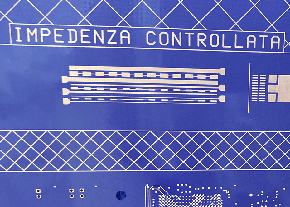
Controlled Impedance
Controlled Impedance.

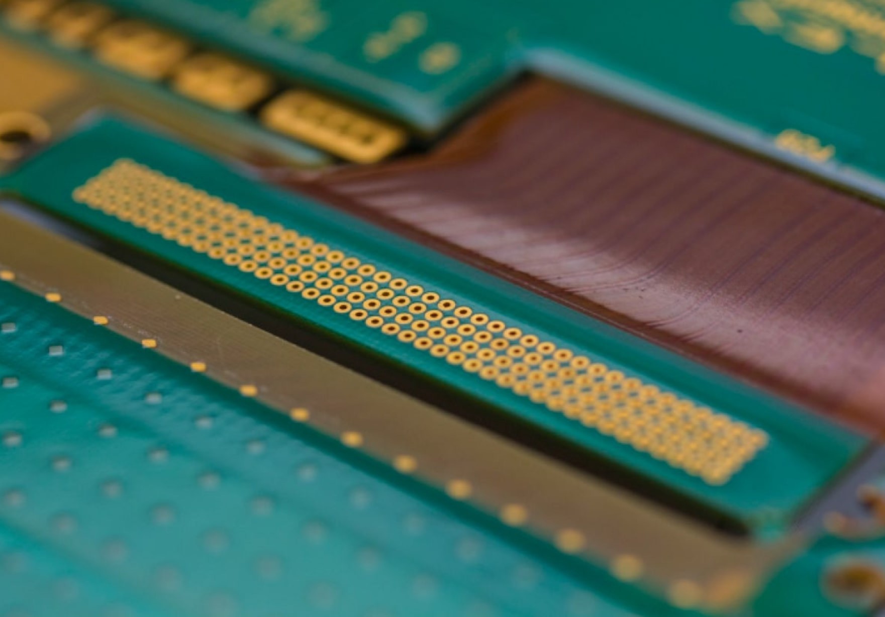
The increase in the signal speed enabled by modern electronic components has forced laminate manufacturers to design and manufacture special materials, capable of ensuring certain and stable behaviour as the operating frequency progresses, while preserving signal integrity.
At the same time, PCB manufacturers have improved their manufacturing process by ensuring that tolerances are progressively narrower and reproducibility is achieved on an industrial scale.
Cistelaier has invested in several areas to support partners in "high speed” projects:
- Polar system for calculation, verification and layup in controlled-impedance structures;
- Genesis Software application for the development of the reference coupon;
- Polar instruments for measuring impedance levels from coupon references;
- control and dosing system for copper plating activation so as not to vary the thickness of the base copper;
- control and dosing system in the acid etching phase in order to ensure a constant process and maintain a tolerance of +/-5% on via size;
- AOI with selective controlled-impedance via control with ability to check dimensional tolerances on specific vias.
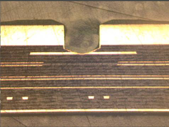
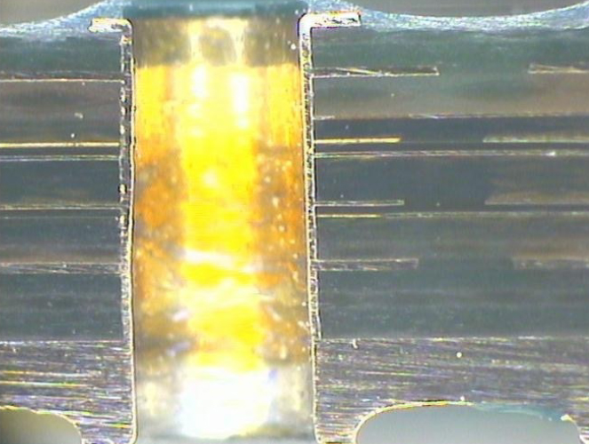
The production cycle of the first batch of each new controlled-impedance printed circuit board has a specific control plan for both the inner layer production process and the pressing process.
The validation of these processes consists in checking the thickness of dielectrics by means of measurements on metallographic sections taken at specific points.
We support you in calculating the correct layup based on your chosen design and material, as well as in selecting alternative materials to ensure the best performance of controlled-impedance PCBs.