Peelable solder mask and EMI shielding
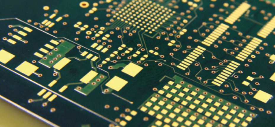
Surface insulation of printed circuits: the solder mask.

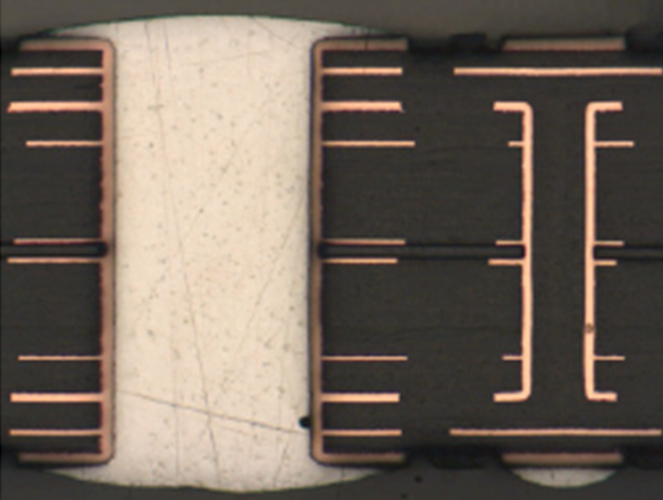
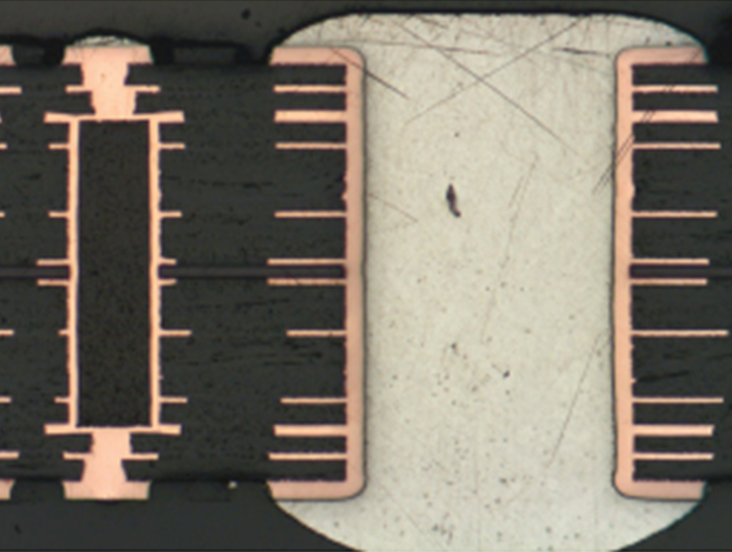
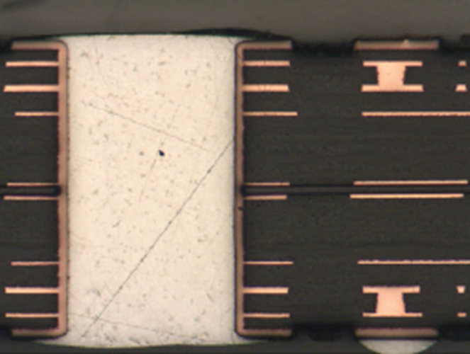
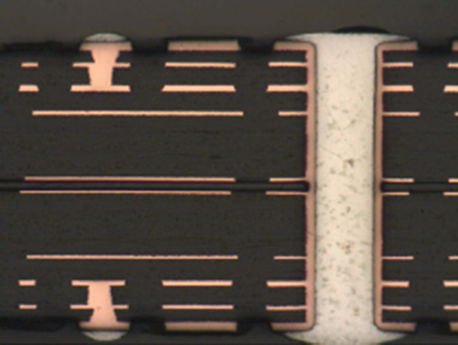
A solder is a polymeric material, similar to paint.
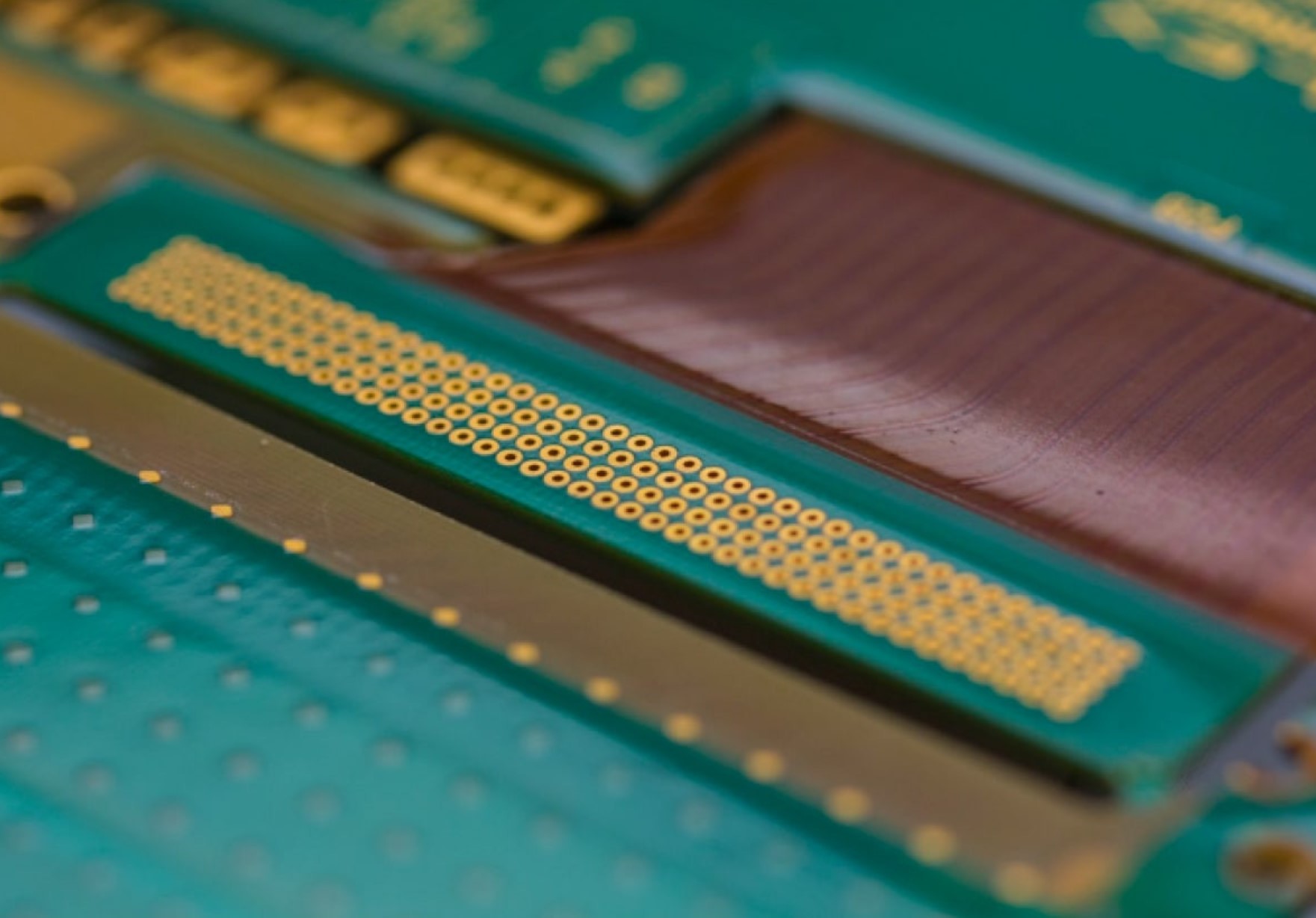
It is deposited via curtain deposition, by screen printing or via spraying, on the external sides of the printed circuit board to protect and insulate the copper vias, from one another and vis-à-vis the external environment, prior to the application of the surface finish.
Exposing the solder to heat creates a genuine protective mask, hence the wording solder mask.
Almost all printed circuit boards are treated with solder, except in rare cases for applications where the solvent, present in the solder composition, is deemed "hazardous".
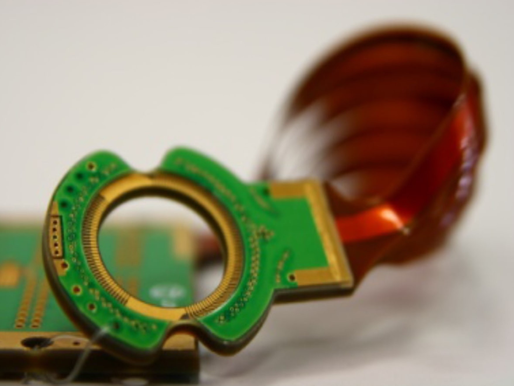
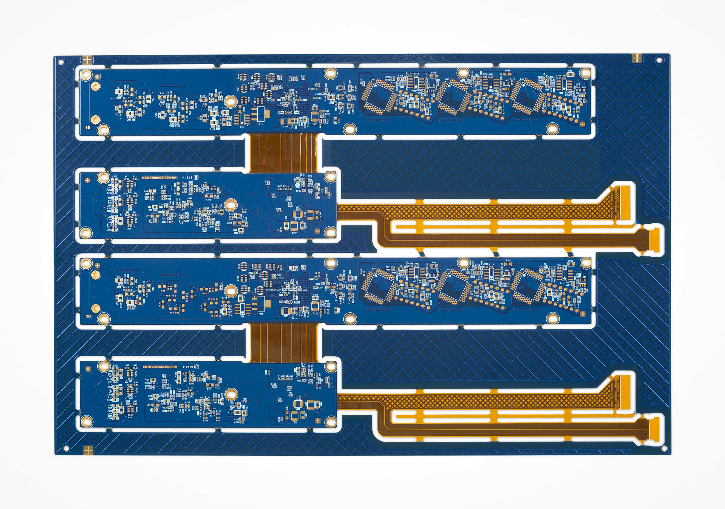
The solder is applied to rigid and flex-rigid PCBs: for the latter, the material used retains, even after heat treatment, the flexibility characteristics required of this category of products.
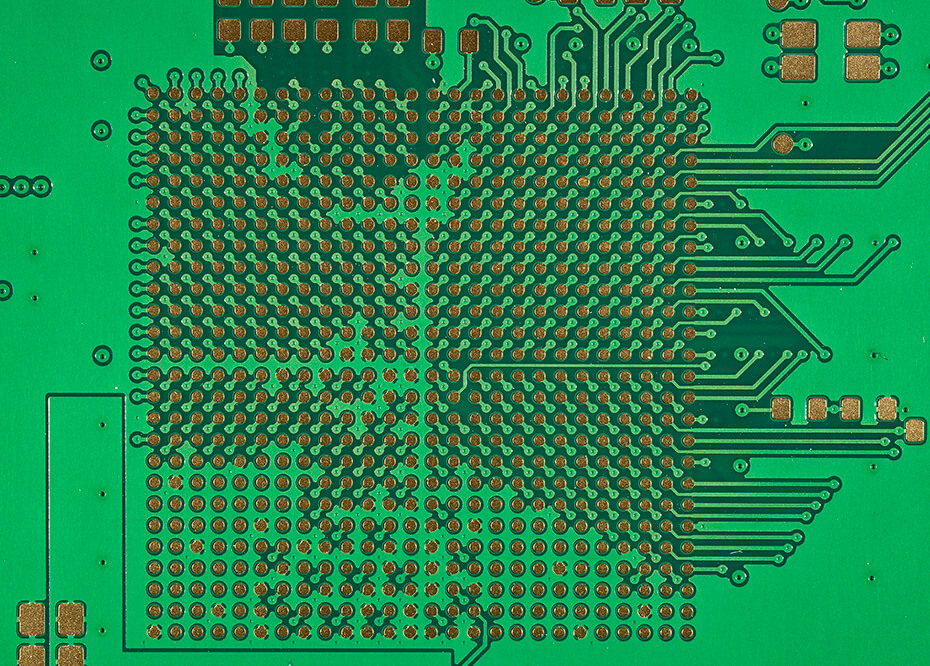
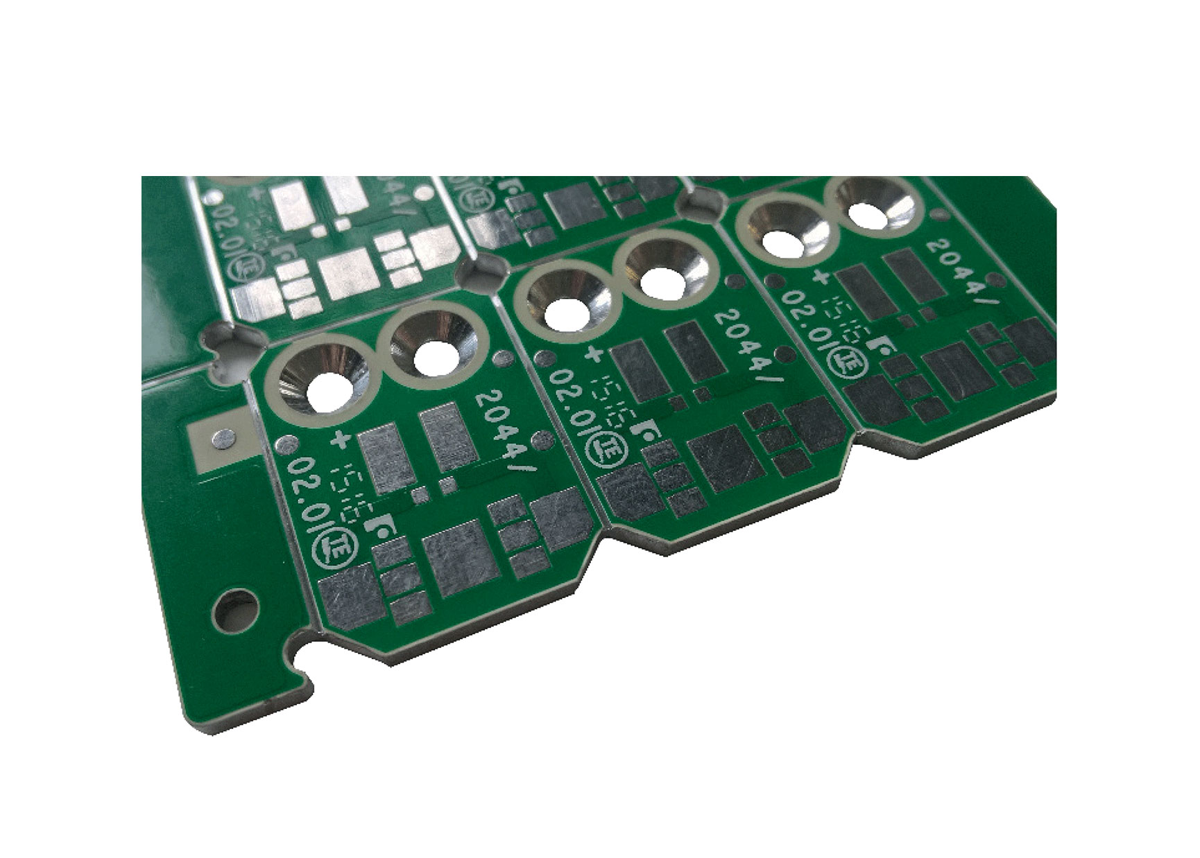
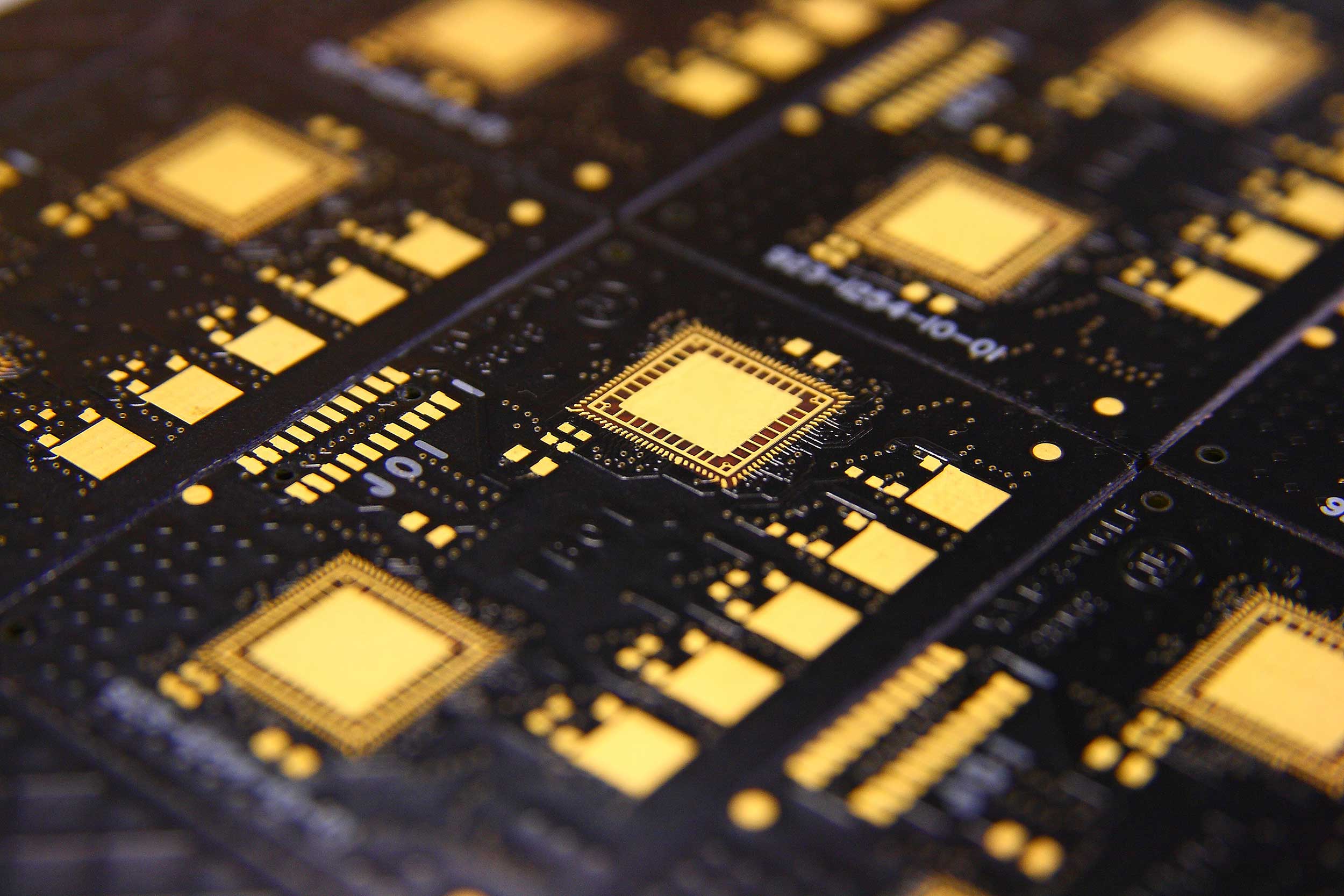
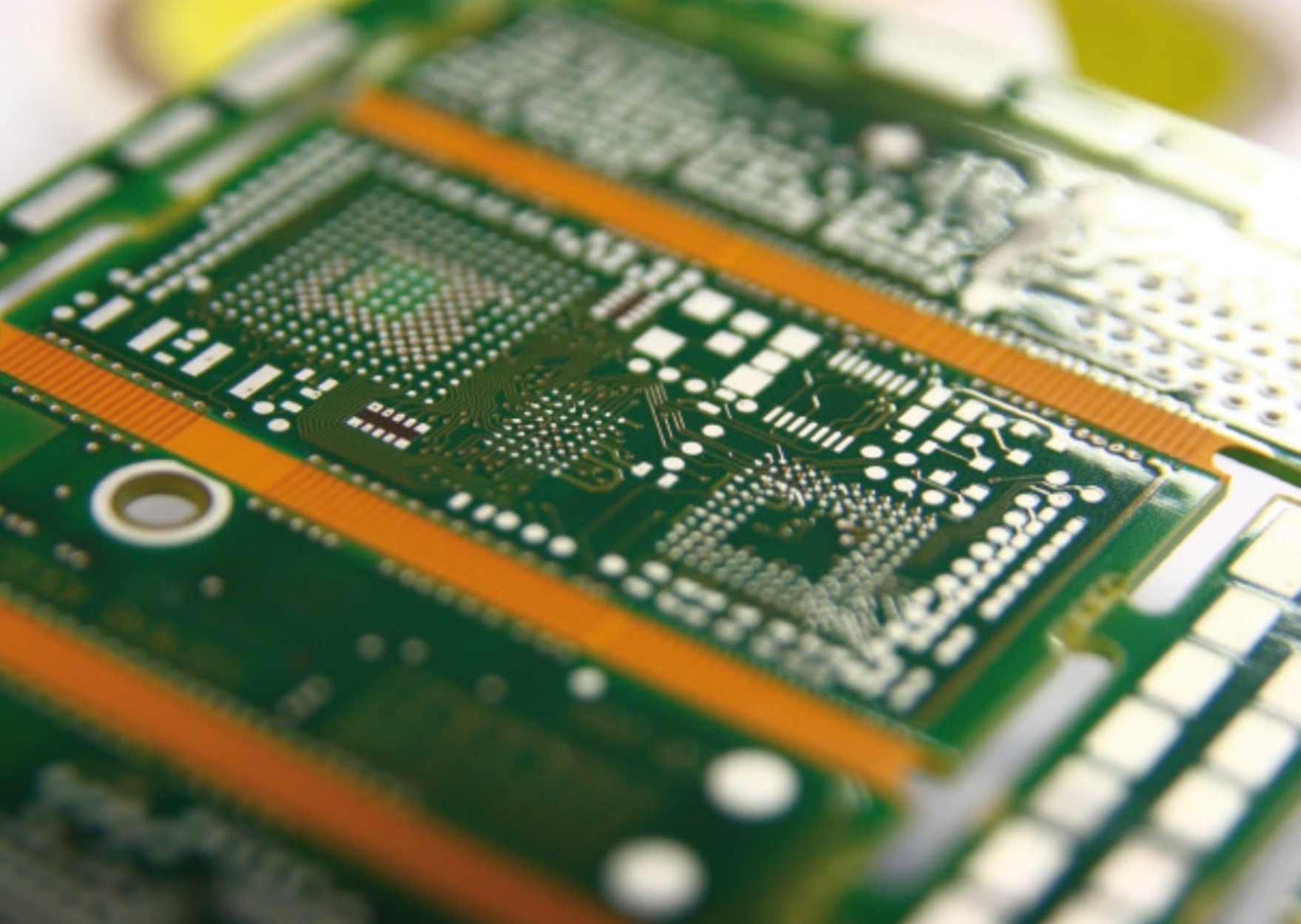
The green solder is the most common because, by way of contrast, it allows more effective defect detection during a visual check.
In general, however, the solder colour does not have a specific function except for some exceptions.
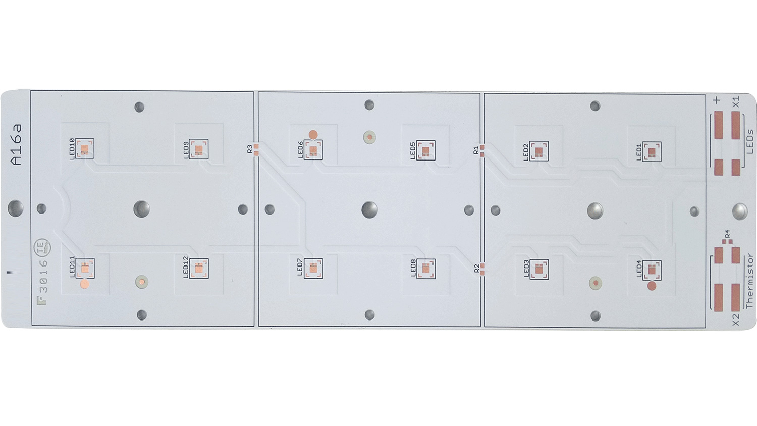
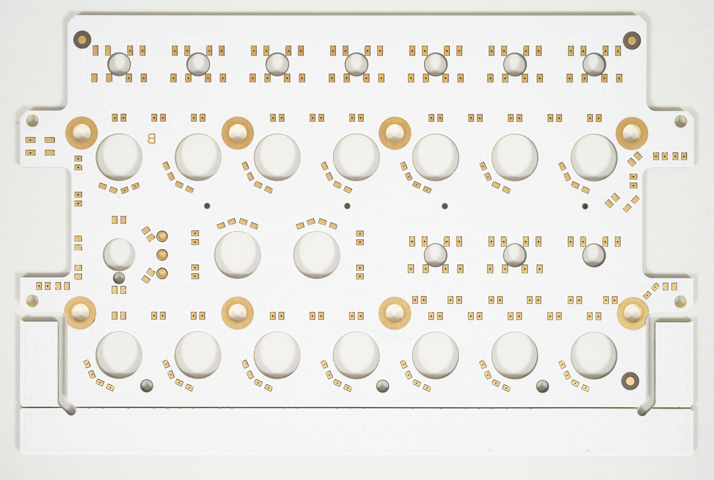
A white solder is widely used in lighting to enhance light reflection, for home LED lighting rather than in the automotive and avionics industries.
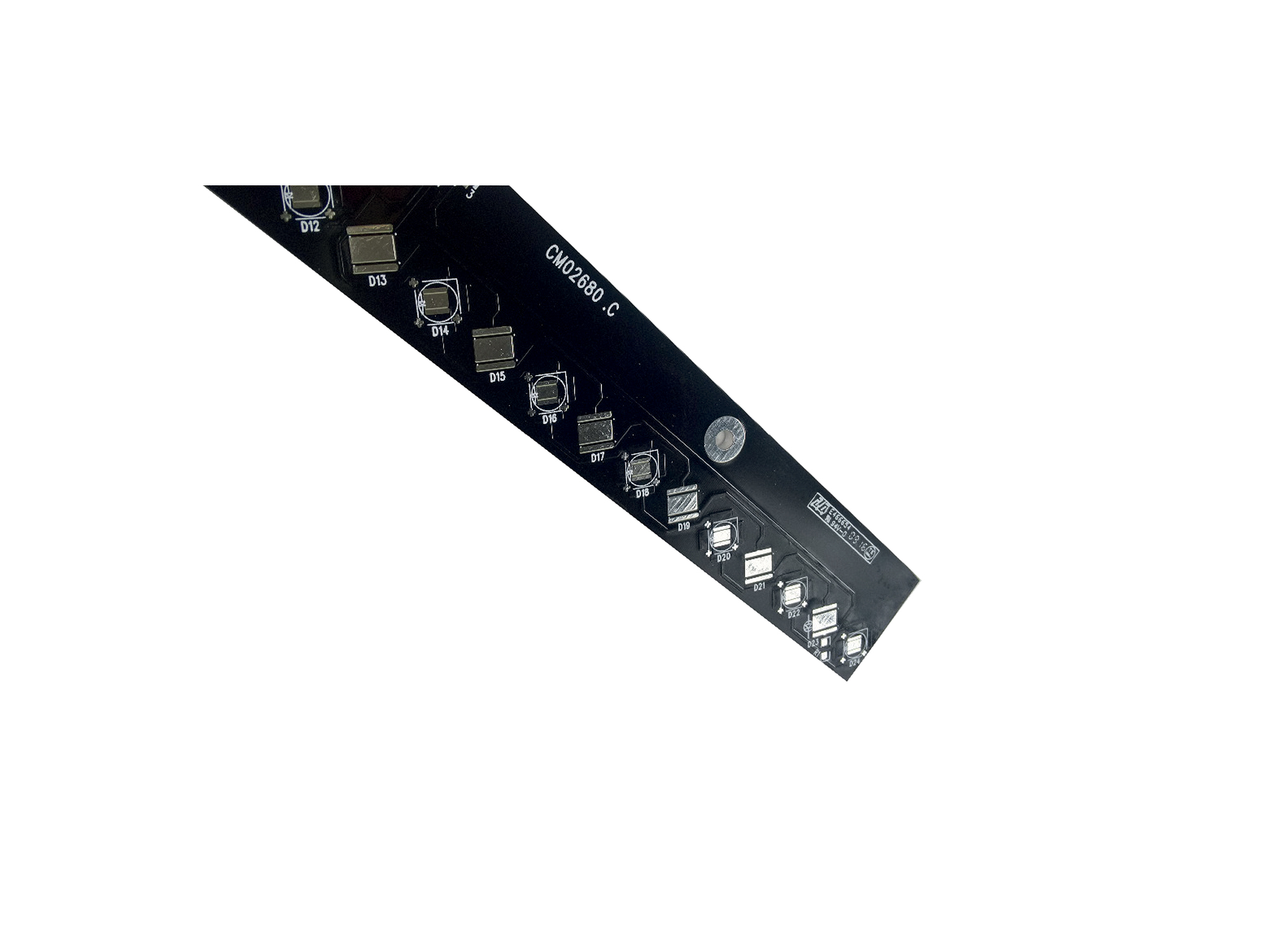
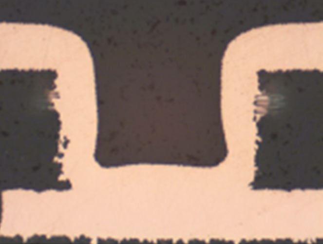
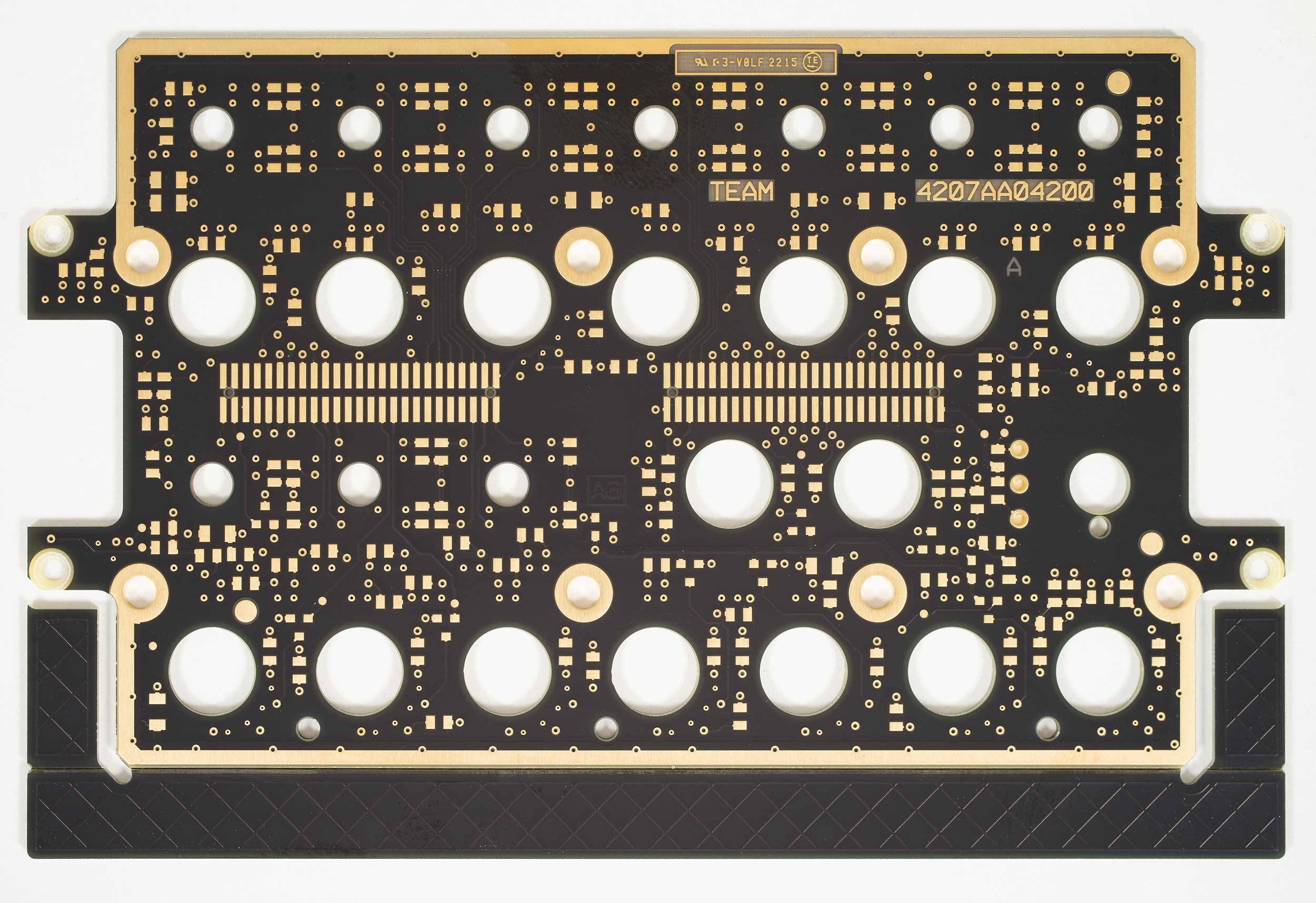
A black solder absorbs light and for this reason it is used in devices such as cameras, barcode readers and other vision devices where light is undesirable.
A blue solder is the one most commonly used for LCD screens.
Our production system for solder application consists of:
- an activation line;
- a state-of-the-art line for solder application via spraying;
- machines for screen printing;
- pre-baking oven;
- exposure machines including an LDI machine for the treatment of the most sophisticated patterns;
and, in particular, but not limited to, to ensure the ideal solder-stop fabrication:
- a development line;
- a baking oven preceded by a UV oven to ensure optimal curing;
- a screen printing machine.
We also have a brushing line for surface treatment after solder capping.
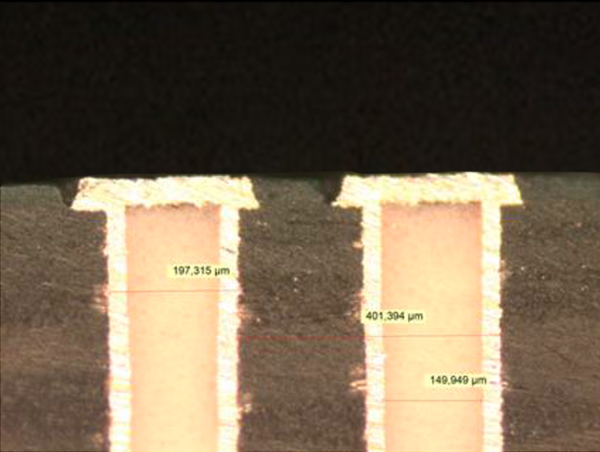
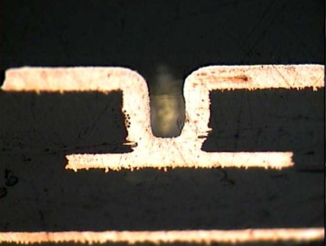
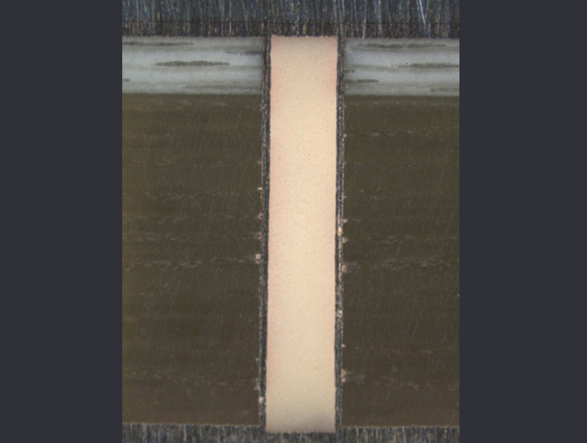
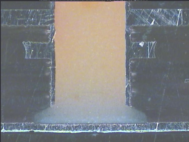
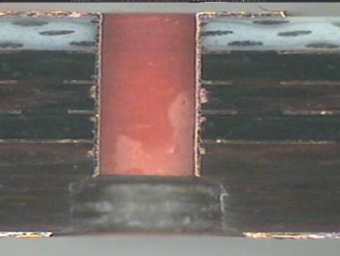
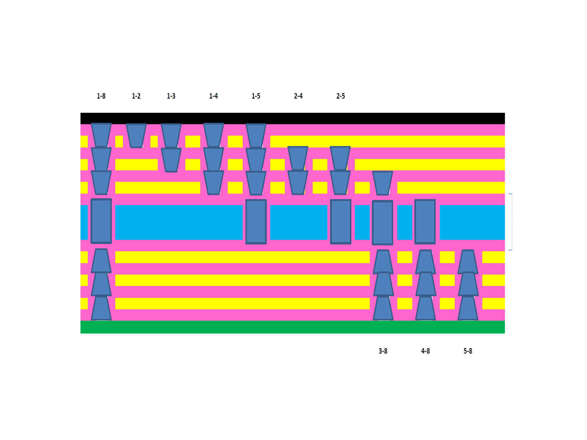
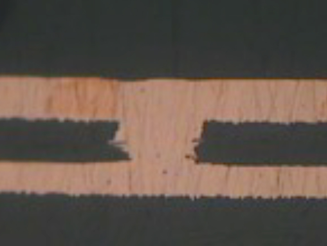
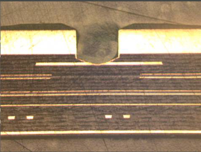
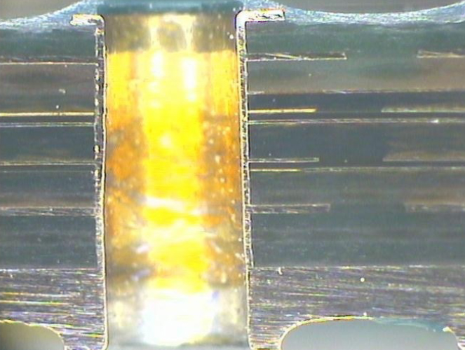
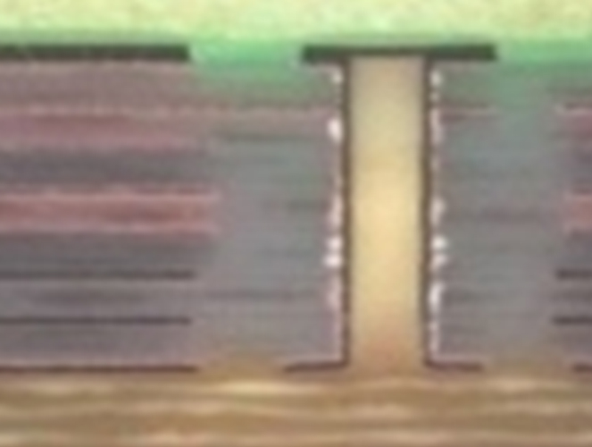
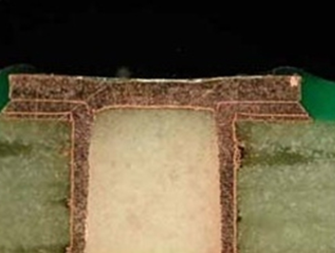
It is the process by which the integral filling or plug-in with solder is carried out in the printed circuit board vias, preventing them from being subjected to the action of weathering.
Portions of the PCB can be covered after application of the surface finish, with peelable solder – the term stems from the fact that it can be peeled off – used to protect the vias or pads from soldering processes.
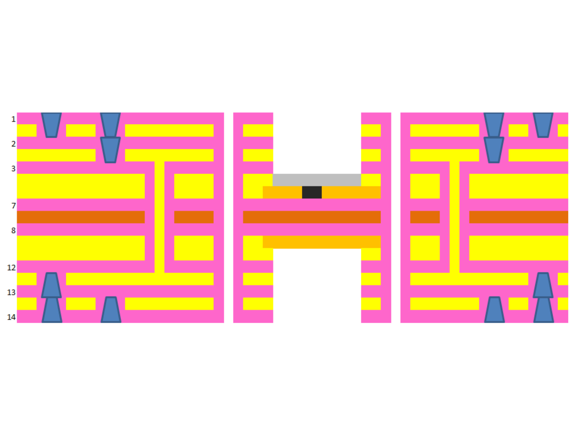
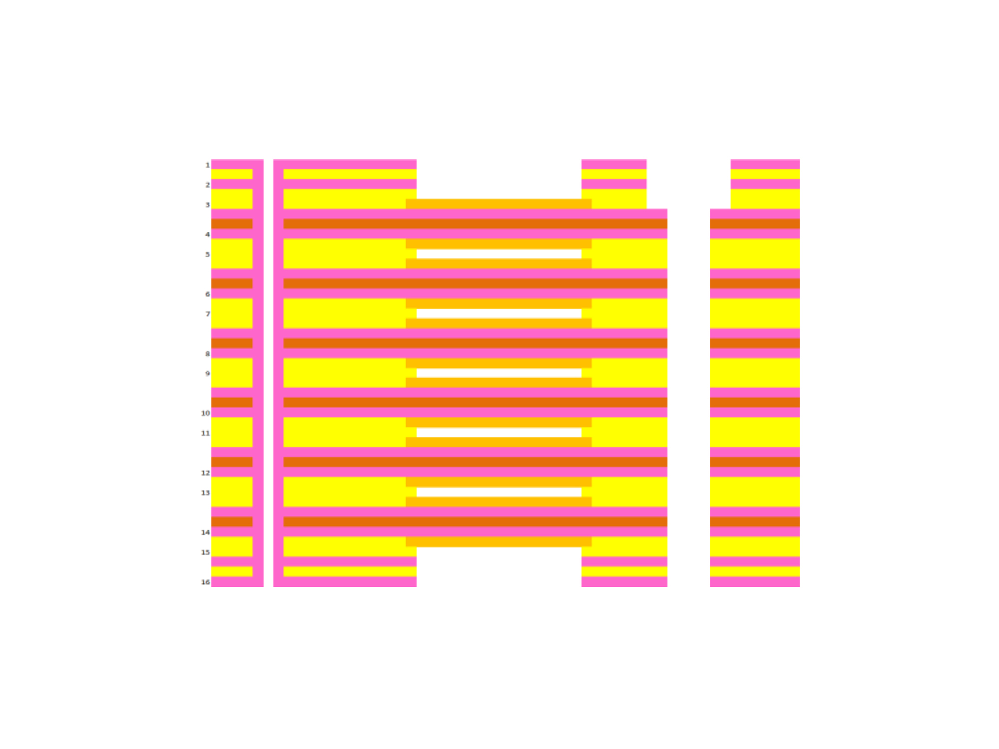
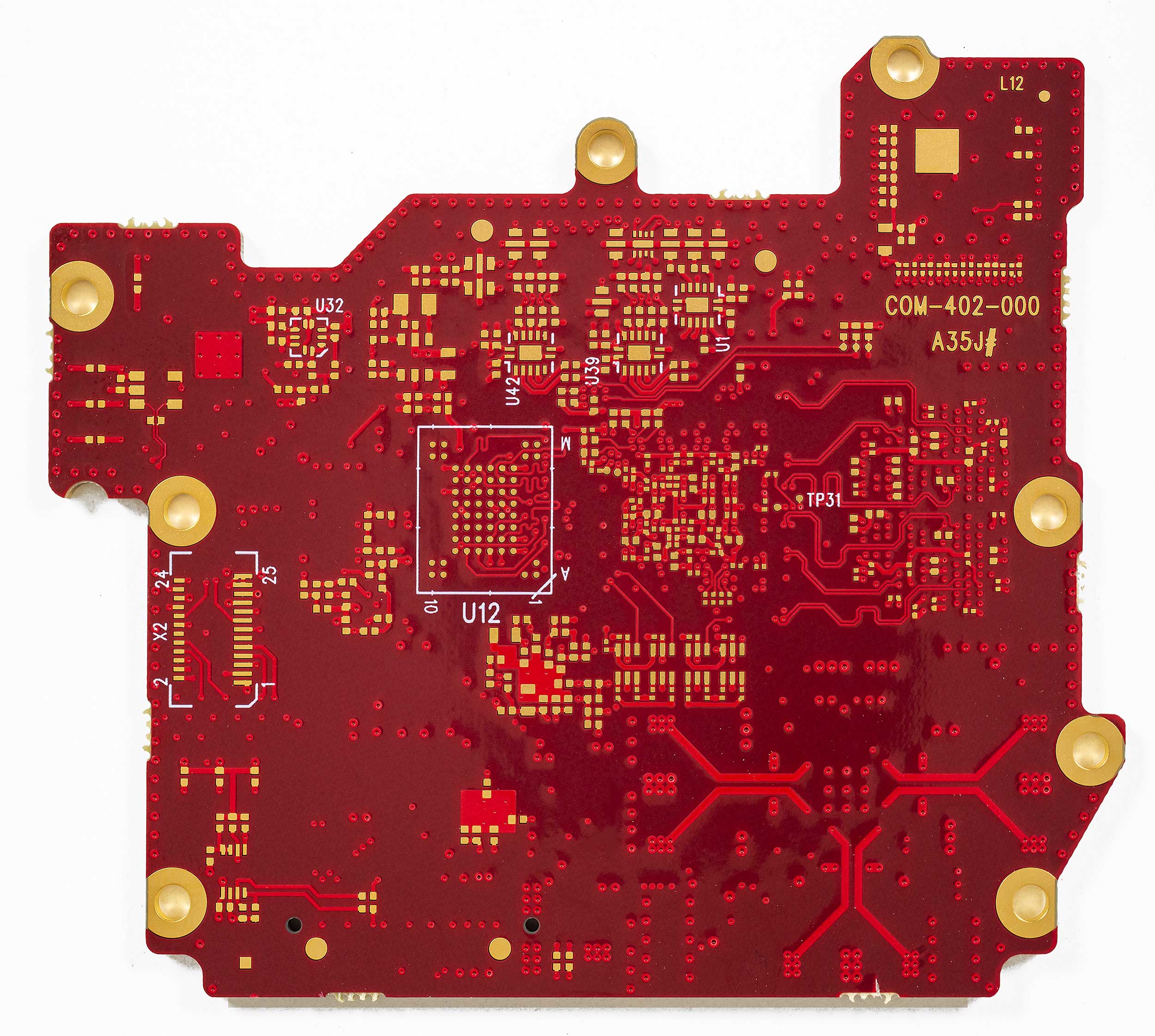
We use all the solder colours available on the market, in glossy and matt finish: green, blue, white, black, red, grey as well as solder in the RAL colour of your choice.
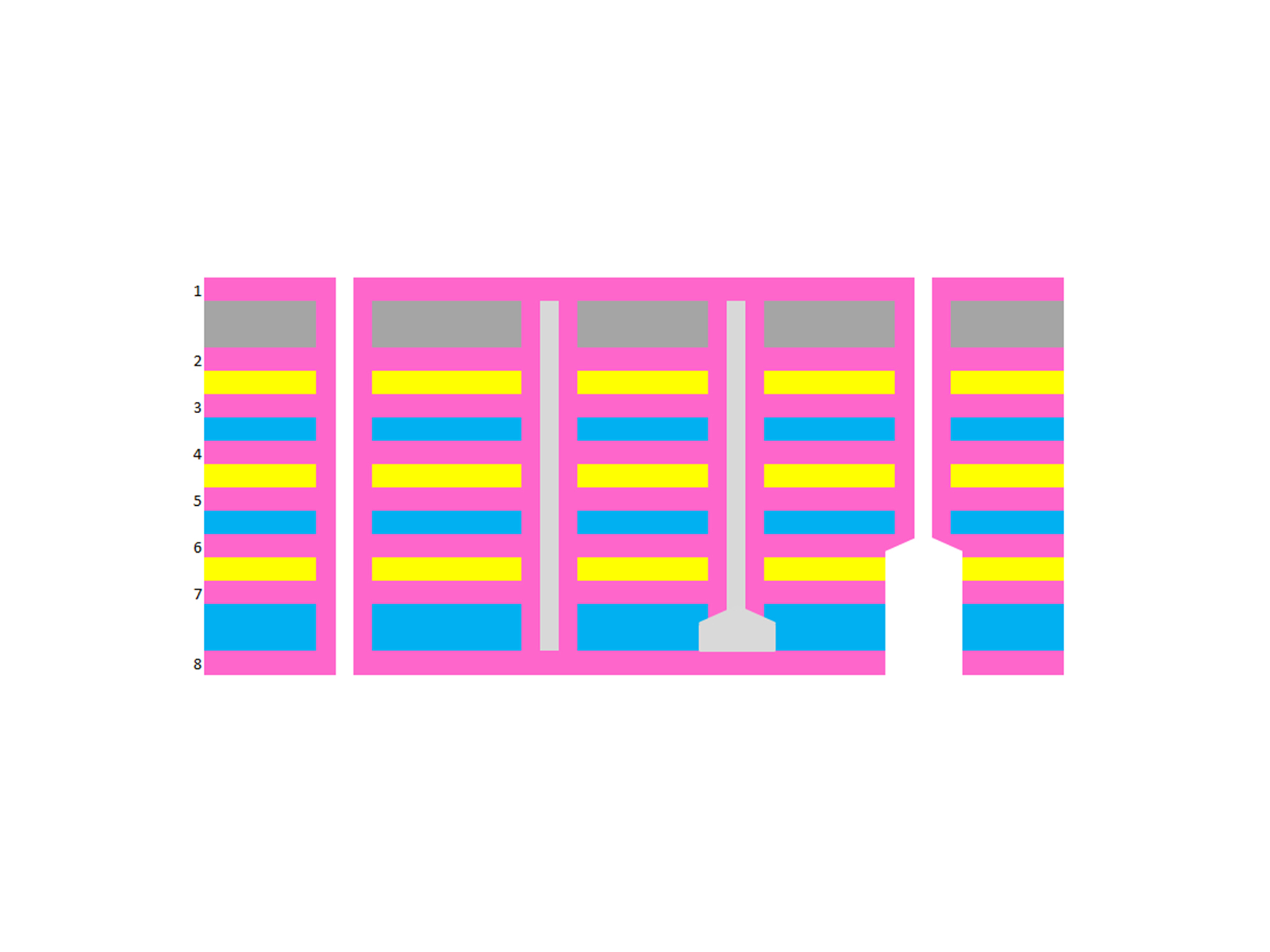
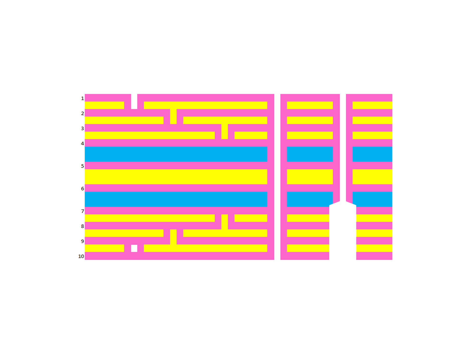
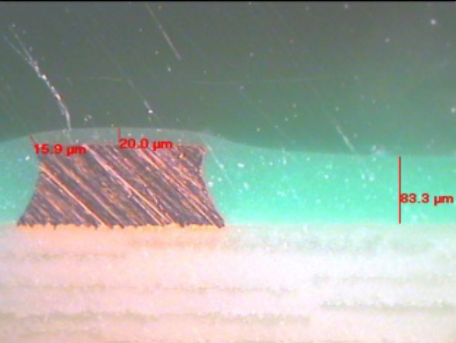
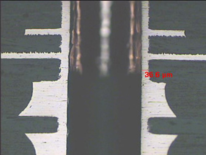
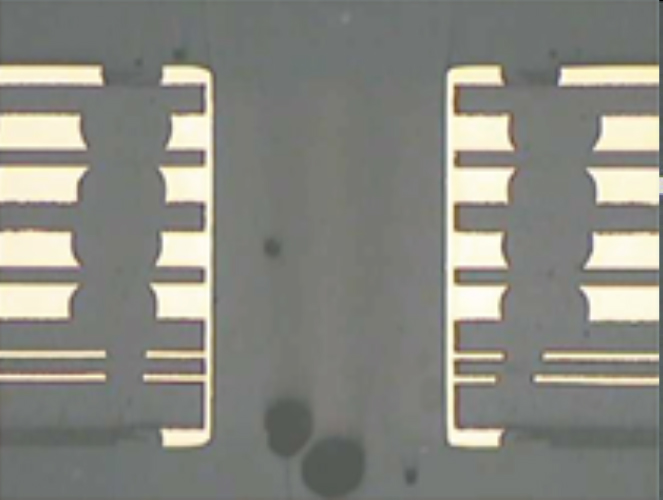
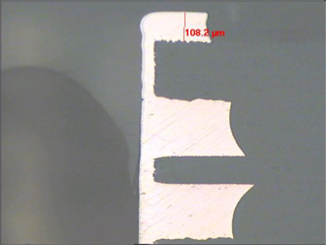
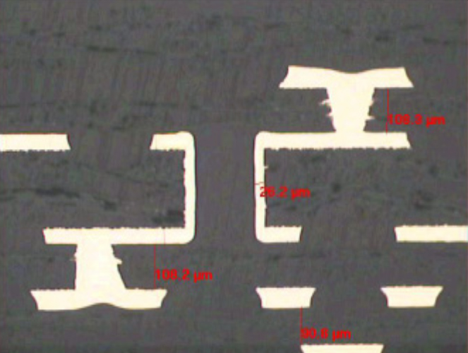
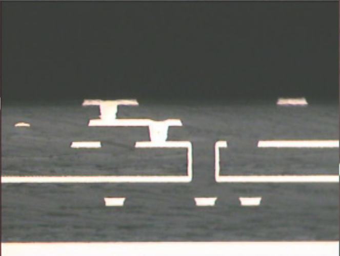
At Cistelaier, our experience and technological equipment allow us to manufacture of thin-trace PCBs as well as high-thickness copper printed circuit boards - or thick-copper PCBs - where the deposition thickness accuracy needs to be maximum.
We use all solutions of solder masking and other masking solutions through the application of thin films for electromagnetic EMI shielding.
Contact us for more information
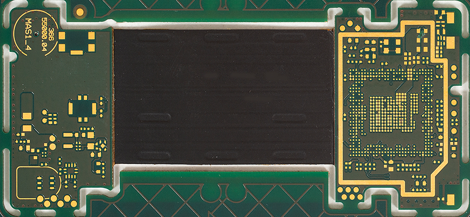
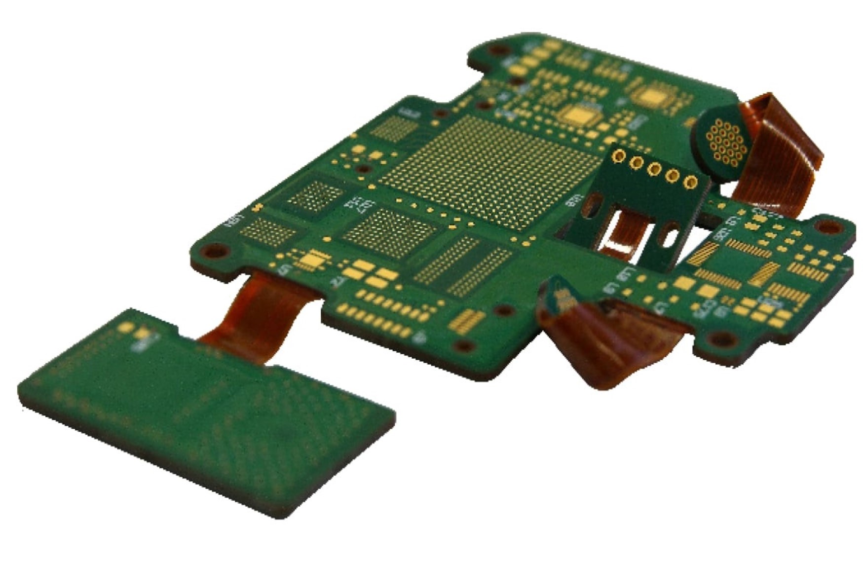
CASE
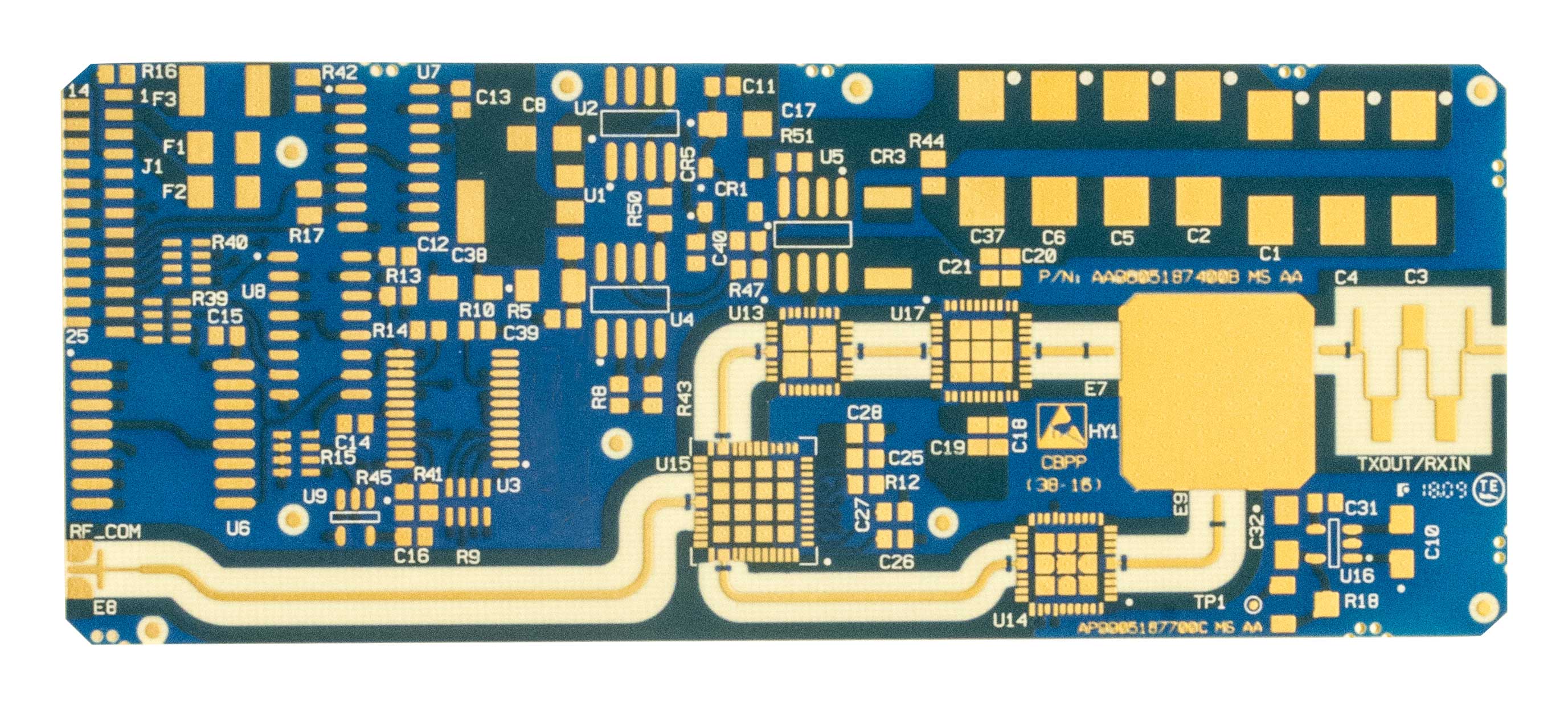
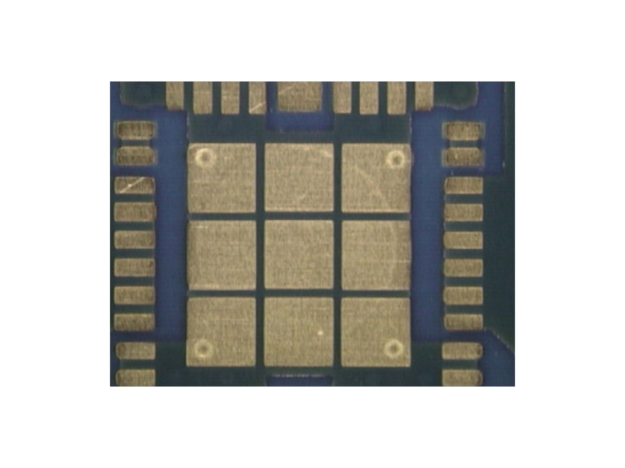
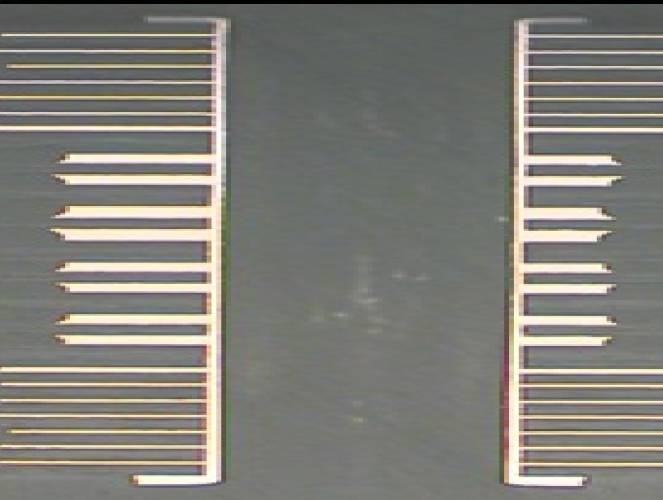
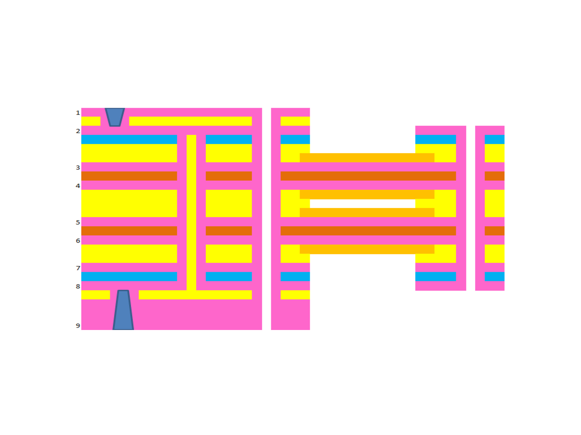
Ml8–Logic + power on same PCB with fine pitch
- Markets:
- PCB Typology:
- Solutions:
- Technologies:
- Materials:
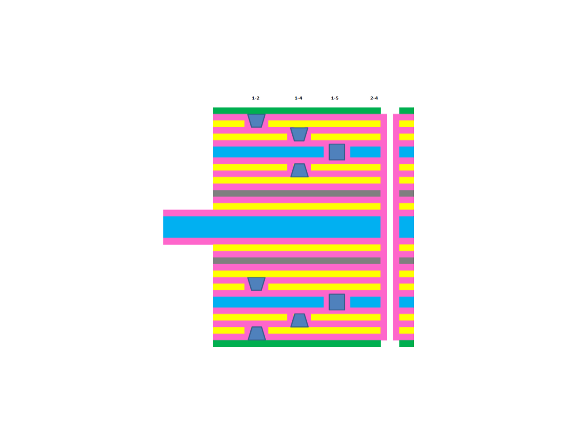
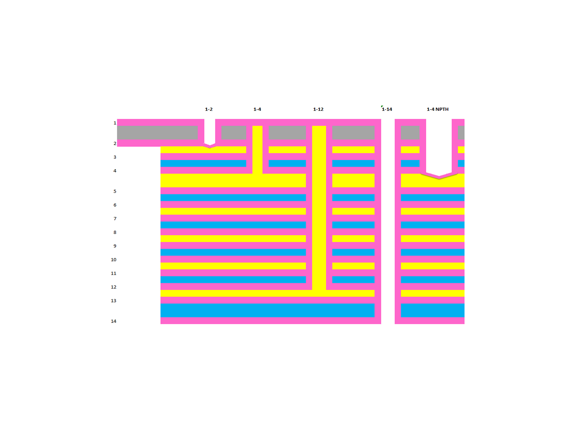
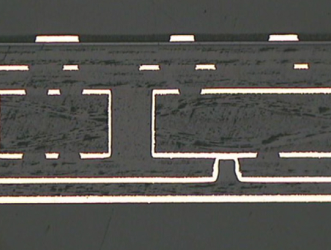
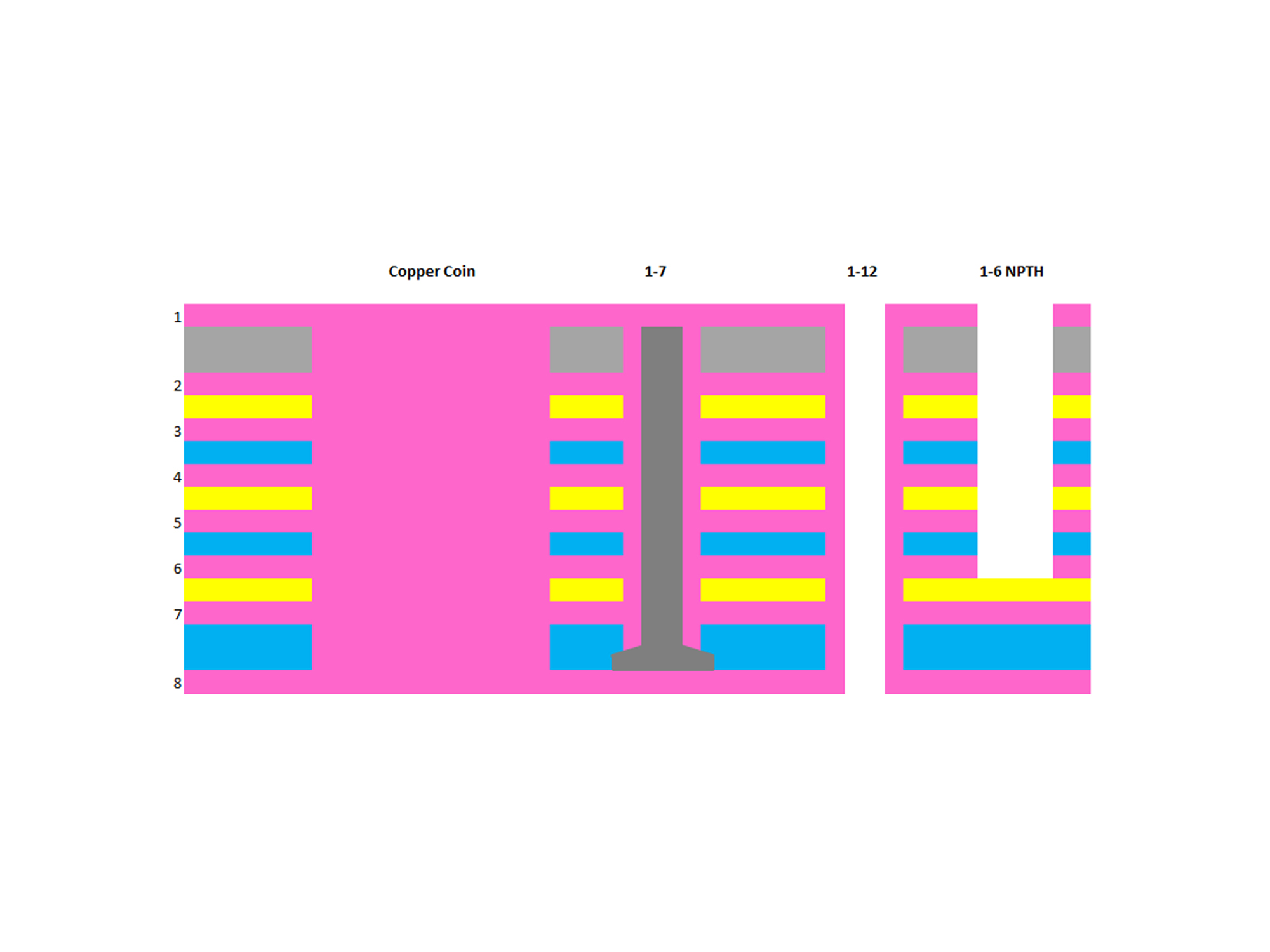
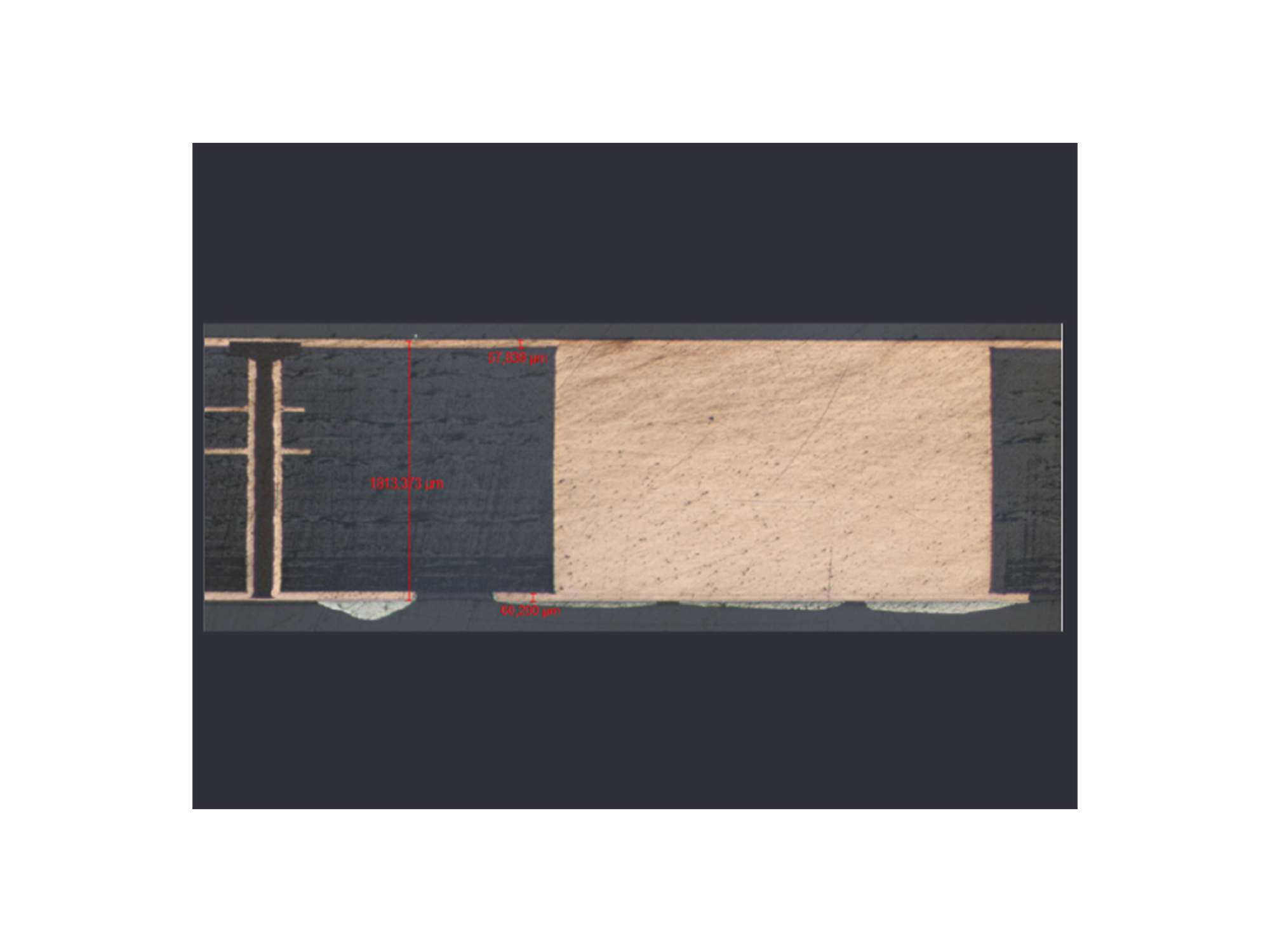
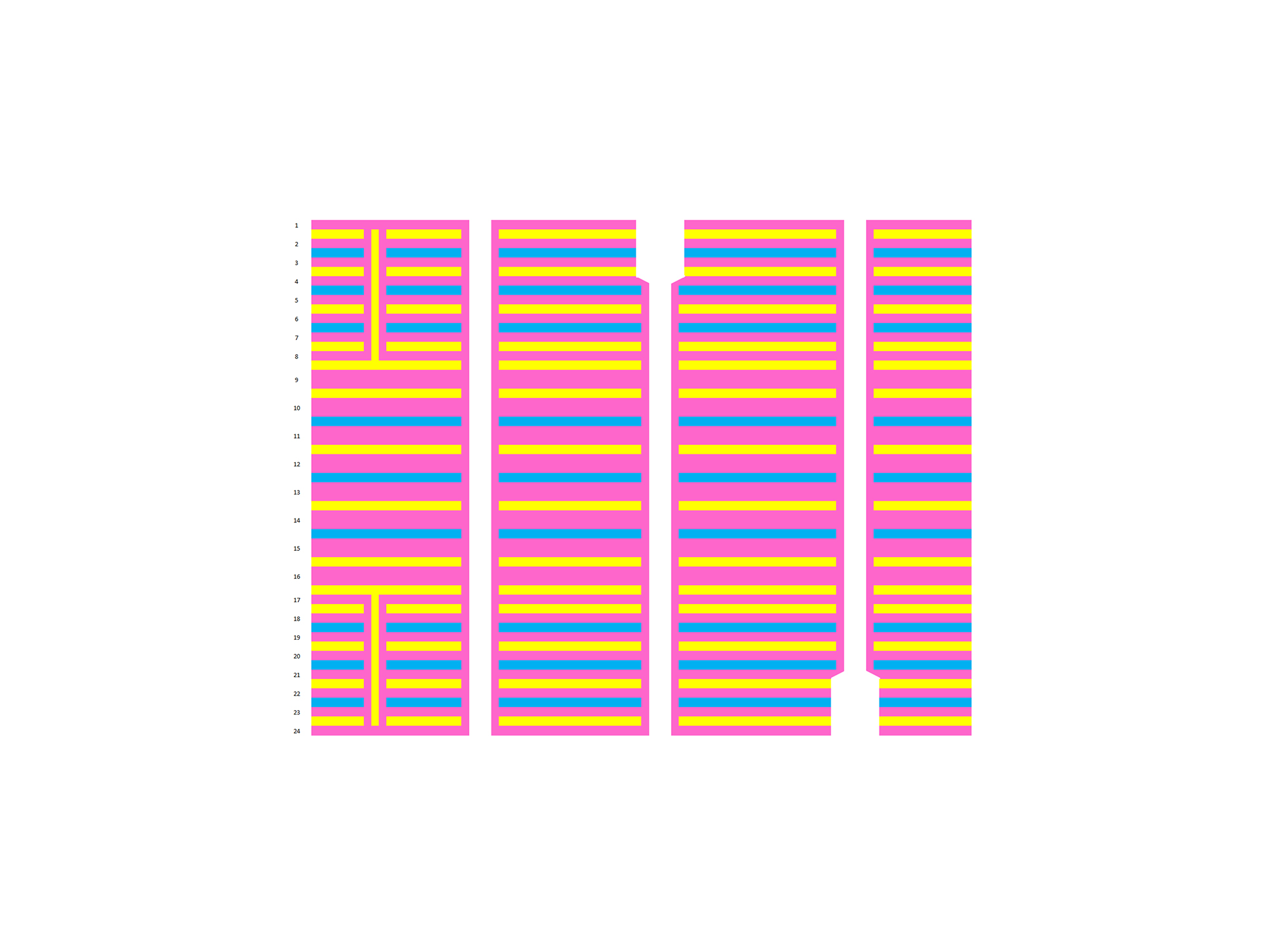
24 layers, 640 mm long x 4.20 mm thickness
- Markets:
- PCB Typology:
- Solutions:
- Technologies:
- Materials: