Vias technologies
Vias technologies

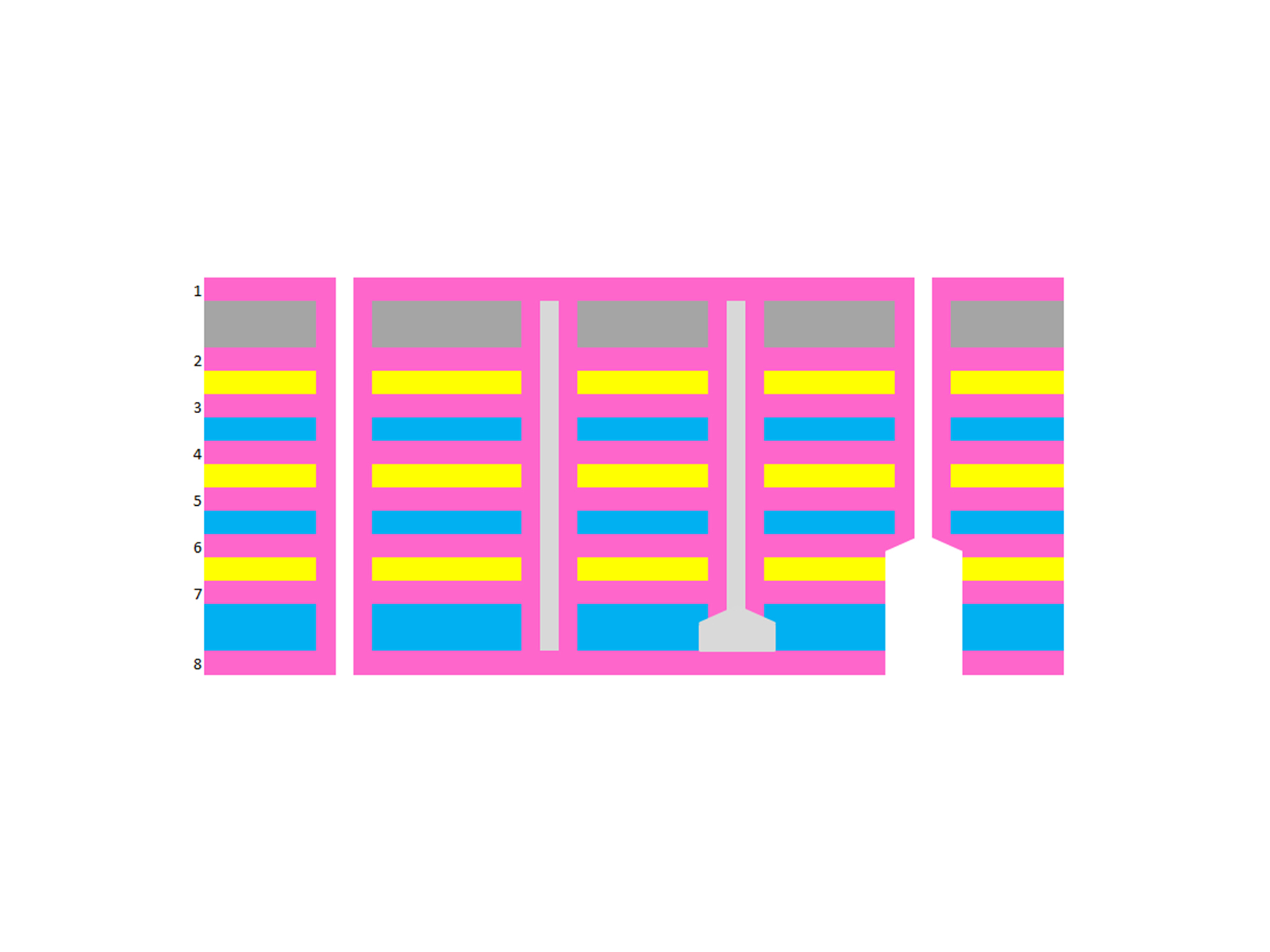
Drilling and subsequent copper plating of the via walls allows different layers of the PCB to be interconnected.
With increasing performance, there is an increasing number of interconnections to achieve, for which it is increasingly necessary to design PCBs with blind vias, obtained by laser drilling or mechanical drilling, or buried or with a combination of both these drilling solutions.
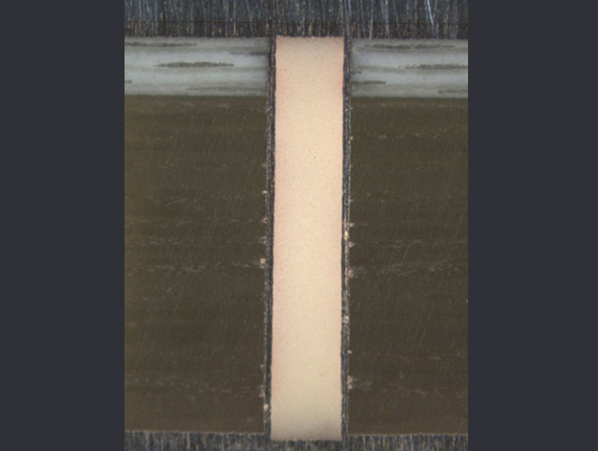
 Blind MicroVias laser 100 µm on Nelco N4000-13 Material
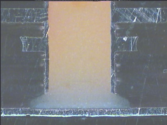
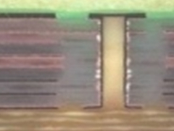
 Blind Vias mechanically made 500mm on Mid TG Material, for heat dissipation in High performance Power Supply.
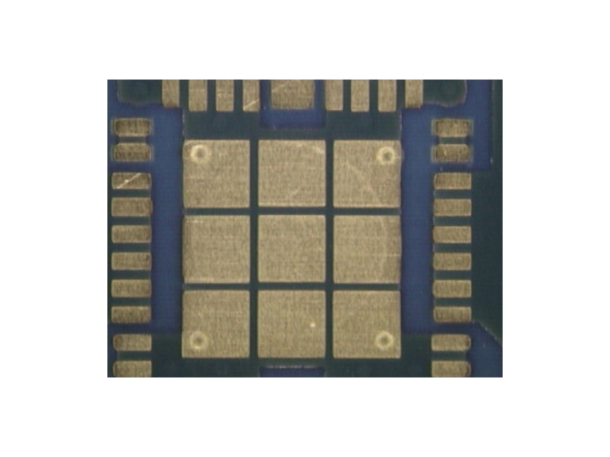
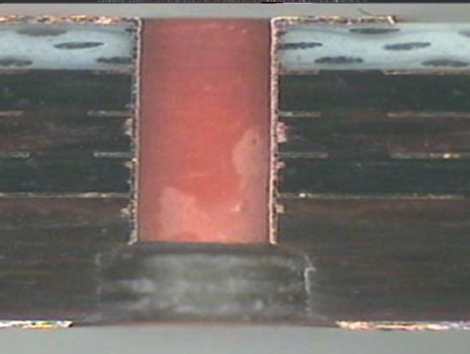
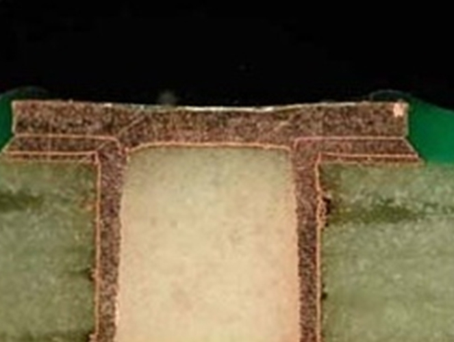
 LASER blind via copper filled
 Blind MicroVias laser 100 µm on High TG 75 µm, copper filled
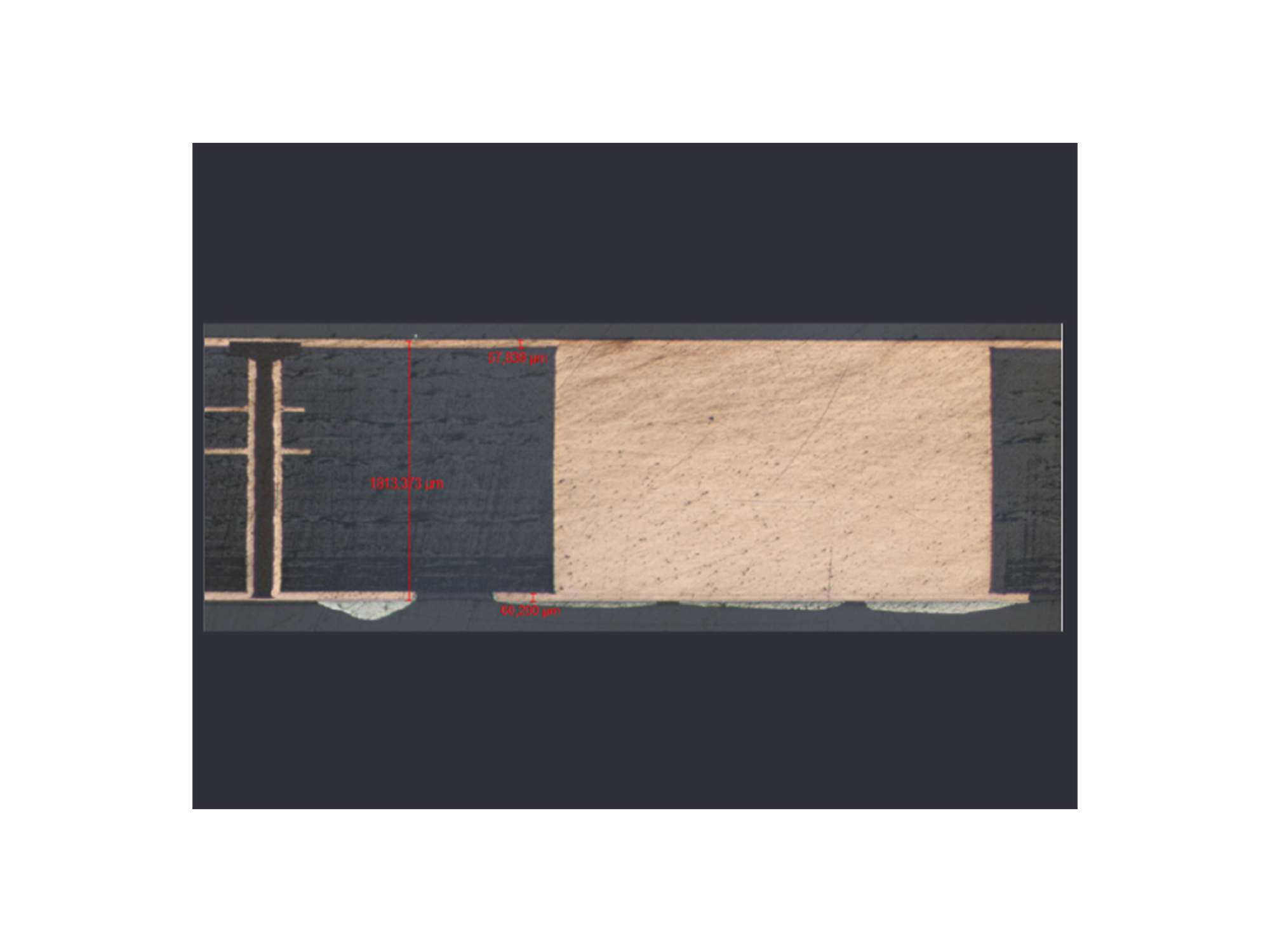
 Copper filled via
At the same time, we are witnessing the evolution of via filling techniques associated with these drilling processes, including copper filling and resin filling, using conductive or non-conductive resins, with and without vacuum application.
The demand for these drilling techniques and the related filling process is growing rapidly as it responds to the need to produce ever higher-performing electronic devices, including PCBs.
This is the case of the HDI PCB.
Here the microvias can be a via-in-pad type for mounting components, staggered or stacked, subsequently filled with non-conductive resins - resin filling - and plated with copper at the top or filled with copper - copper filling - and plated with copper to obtain filled and capped vias.
 Blind MicroVias Laser 75 µm copper filled, stacked vias and burried vias.
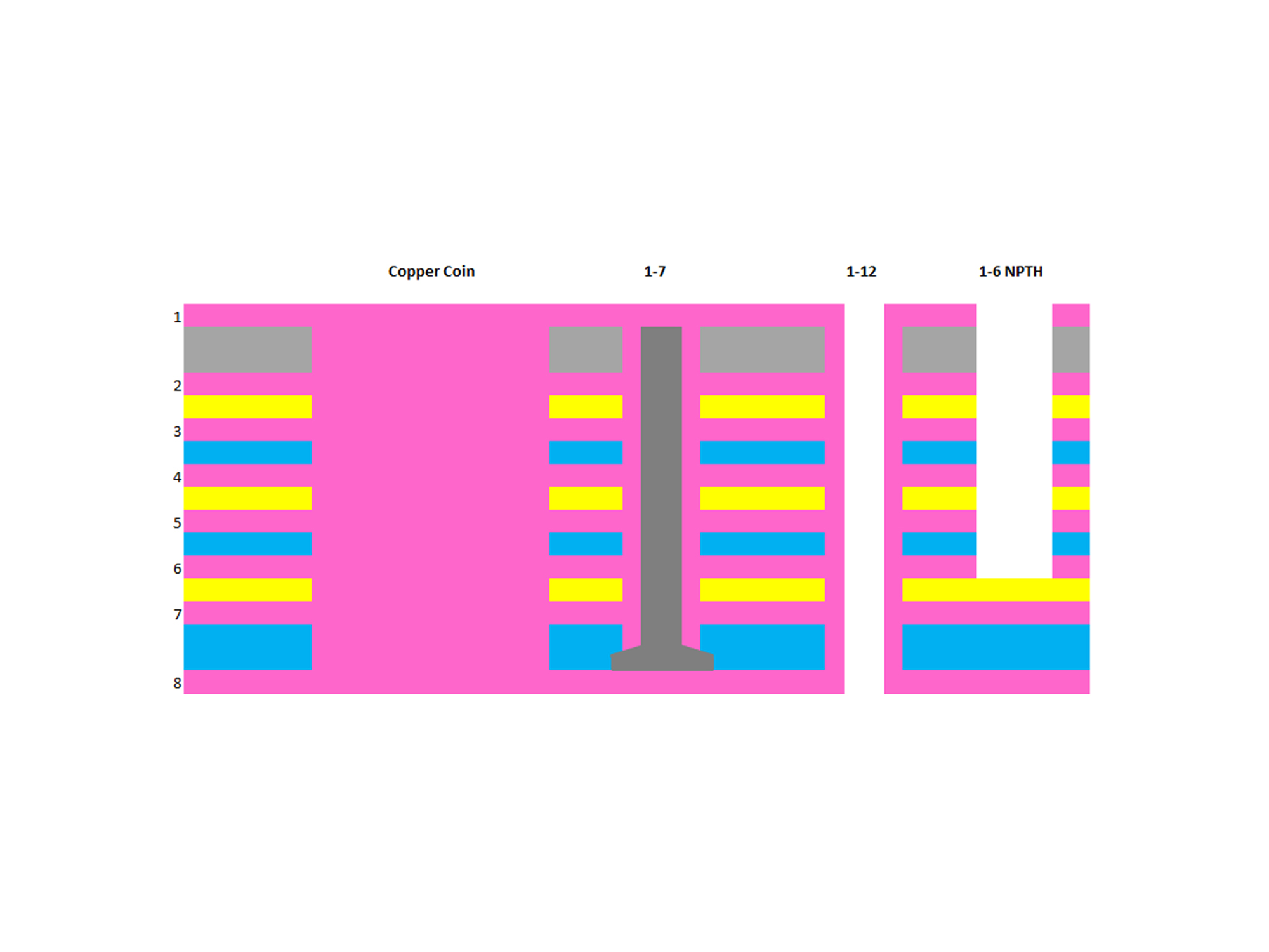
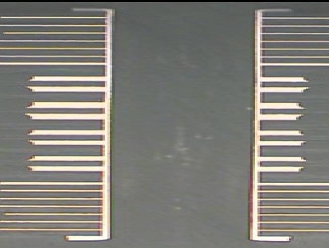
 Stacked vias
 Staggered vias
 Filled & capped vias
 Filled & capped vias
 Resin filled and capped vias
 Blind µvia laser 100µm on Nelco N4000-13 material
Reverse build-up technology can also be used to ensure that the pads are perfectly level.
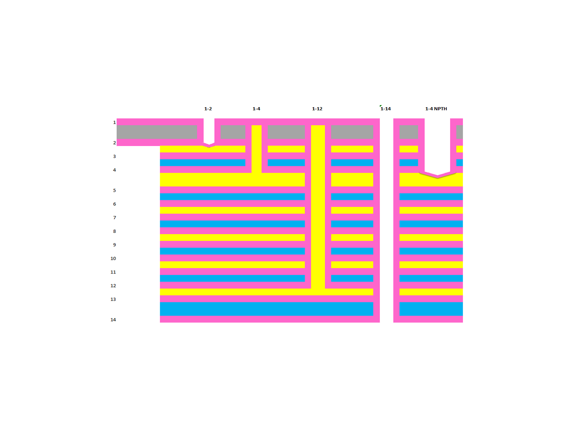
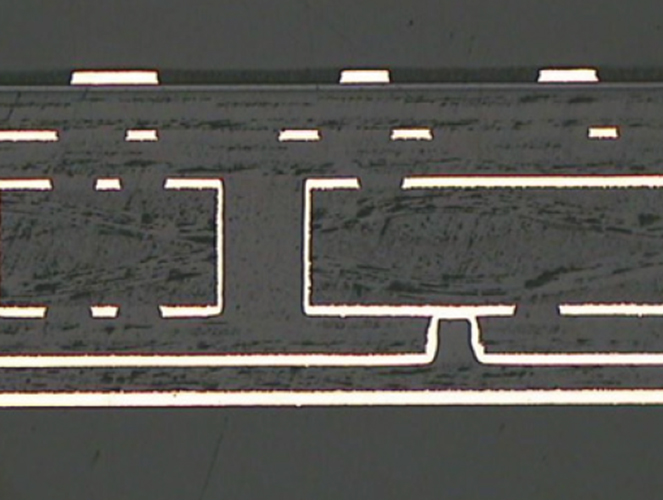
Where the effects of signal interference need to be minimised, along through holes, the back drilling technique can be used for these vias, which removes the unnecessary portion of copper plating.
We have the experience and tools required to handle all the drilling techniques used in PCB fabrication.
Here are some examples.
 Blind MicroVias laser 100 µm on High TG Material, copper filled: SBU 3+N+3
 Sequential build-up 2+n+2; Laser vias from layer 1 to layer 3:125 µm; Insulation layers 2x60 µm.
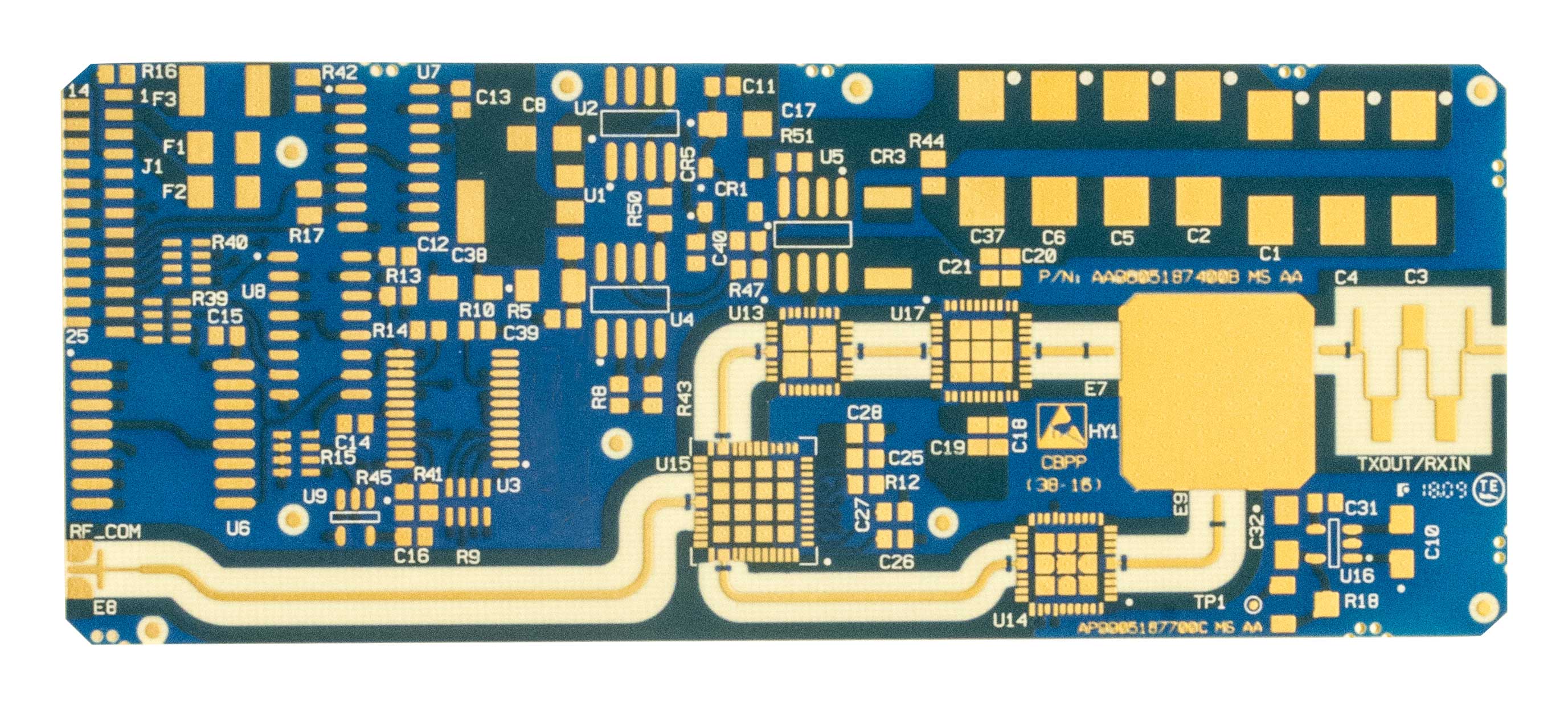
 Sequential build-up 4 layer Rigid Flex: Blind Vias mechanically made on mixed Layup Boards: Ro4350+High TG material.
Rely on us to find the right solution for your PCB.
Contact us for more information
CASE