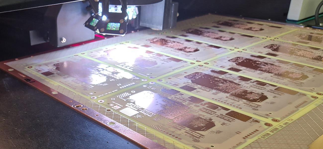
Inner Layer’s Automatic Optical Inspection (AOI)
Even if it is not enough, as we all know “A good start is half of the job!”.
What could help to start in the very best way the process to manufacture a PCB is to combine SPC together with Automatic Optical Inspection to make iterative improvements when and where necessary.
In our last article we described the inner layers etching process, from dry-film development to copper etching and to residual dry film stripping so to get an etched inner layer ready to take part in the PCB stack up.
As we said, to optimize the result of that process it is necessary to keep stable both, the conditions of the etching process itself and the conditions related to the previous processes of inner layers lamination and imaging.
After that, the good common sense, even before the IPC norms obligations, suggests to inspect the etched inner layers. Nevertheless, according to the IPC norms, inner layers must be 100% inspected after the acid etching process.
On the practical level, the AOI is a comparison of the inner layer drawing to the real and concrete inner layer after the acid etching process. To reach this result, it is necessary to load in the AOI machine the drawing of the inner layer to be inspected and the acceptability tolerances on the different geometries like pads, tracks, distance, embedded resistors and profiles (mainly in case of microwave structures). The tooling area is in charge to deliver the drawing to the AOI department, so to allow them to perform the AOI.
The AOI process is based on acceptability rules normally defined in a control plan. This document is populated with customer requirements/specifications and/or other norms adopted in the PCB sector.
Here following a list of the most common specification used in the world:
- IPC-A-600
- IPC 6012 for rigid PCBs, IPC 6013 for flex and rigid-flex PCBs and IPC 6018 for High frequency and Microwave PCBs
- IPC specific addendum for critical final use sectors like Space, Automotive and Medical
- ECSS-Q-ST-70-60C for Space applications
The objective of this inspection is to find all deviations to conformity so to suggest which adjustments are necessary to the inner layer’s lamination and imaging processes as far as to the acid etching process to reduce scraps and, if any, to detect them as soon as possible so to avoid spending additional hours and money to produce something “scrapped” since the beginning.
If you want to learn more about the PCB manufacturing process, feel free to contact us!