PCB’s production process
PCB’s production process requires wide and deep multidisciplinary knowledges referring to material properties, to photoprint, electronic, mechanic, chemistry, electrochemistry and many more than those related to specific applications, meaning properties referred to the final product of which the PCB will be part.
To manufacture a printed circuit board, you furthermore need machineries, production lines and instruments for process and product control, making this knowledge intensive activity also a capital intensive one.
With this article and the following ones, which we will send out on a monthly basis, we intend to provide the rudiments useful to better understand the production steps required to manufacture printed circuits boards.
For this purpose, we will use a basic manufacturing process for the production of a multilayer printed circuit.
Here below we will limit ourselves to indicating the sequence of the main production phases that we will describe in more detail in the next articles.
- Inners activation and dry-film lamination
- Inners Direct Imaging
- Inners development, Copper etching and dry-film stripping
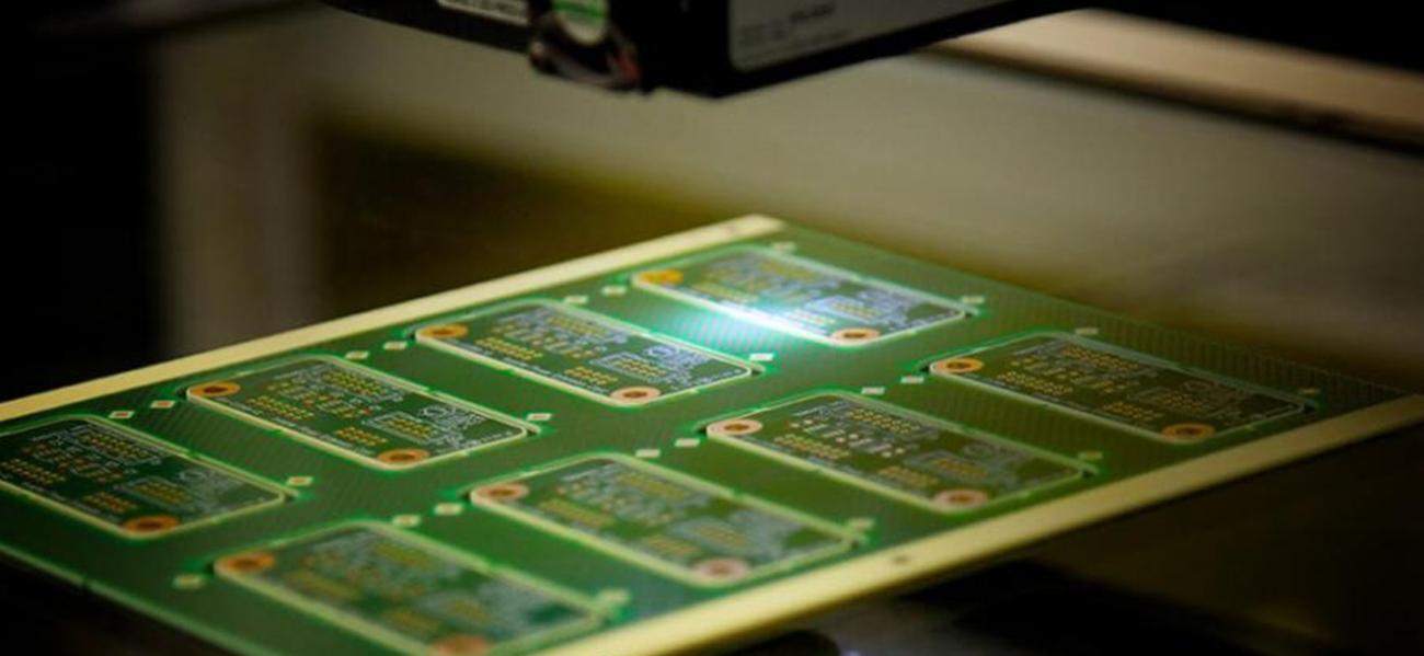
- Inners Automatic Optical Inspection (AOI)
- Inners Punching
- Inners preparation and drying before pressing
- Build-up preparation and pressing
- Xray checking, drilling and brushing
- Chemical & Electrolytic Copper holes plating
- Outers activation and dry-film lamination
- Outers Direct Imaging
- Outers Development
- Electrolytic Copper and Tin surface & holes plating
- Outers dry-film stripping, Copper etching and Tin stripping
- Outers Automatic Optical Inspection (AOI)
- Outers activation and solder mask deposition
- Solder mask Direct Imaging and Development
- Finishing – Chemical Gold plating, Electrolytic Gold plating, Chemical tin plating, Silver plating, Copper Oxide Passivation, HASL, Tin-Lead
- Routing and Scoring
- Mechanical inspection
- Electrical test
- Microsections preparation and verification
- Final optical inspection
- Baking, packaging and shipping
As previously said, even for products considered to be of standard technology, a lot of manufacturing steps are required that involve the use of no less than 30 different machines and production lines as well as suitable environments by temperature, humidity and cleaning.
The comprehension of production technology even by PCB’s designer side, allows to optimize the design for manufacturing & testing with an impact on in place PCB effectiveness and on related costs, as well as on the subsequent assembly phases of the electronic components.
In the next articles we will better clarify the peculiarities and complexities of each single step.
Let’s follow us on our blog!